Fermi Level In Semiconductor / Fermi Energy And Fermi Level Definition Applications Formula. Due to lack of sufficient energy at 0 kelvin, the fermi level can be considered as the sea of fermions (or electrons) above which no electrons exist. The fermi level represents the electron population at energy levels and consequently the conductivity of materials. The fermi level is referred to as the electron chemical potential in other contexts. The fermi level is the surface of fermi sea at absolute zero where no electrons will have enough energy to rise above the surface. Fermi level is a kind of measure of equilibrium electronic energy of a solid material.
This is one definition and if we apply concept of fermi level in semiconductors we say it is an energy level between the forbidden band gap (where no electron exists as per the definition) where only the probability is 50%. Primer on semiconductors unit 5: However, for insulators/semiconductors, the fermi level can. Smith context the first part of this lecture is a review of electrons and holes in silicon: Kb is the boltzmann constant.
Quasi Fermi Levels Explained Youtube from i.ytimg.com Fermi level in extrinsic semiconductors in an intrinsic semiconductor at t = 0 the valence bands are filled and the conduction band empty. However as the temperature increases free electrons and holes gets generated. Primer on semiconductors unit 5: A semiconductor is a solid that is defined as having its fermi level (chemical potential) in a band gap of the electronic structure of the solid, which is not too large compared to the thermal energy, so that, according to the fermi distribution, at room temperature you have a significant number of electrons and/or holes in the conduction and valence band available for conduction. The value for the fermi energy and carrier density is obtained at the crossing (indicated by the arrow) of the two black curves which represent the total positive and total negative charge in the semiconductor. The fermi level is the surface of fermi sea at absolute zero where no electrons will have enough energy to rise above the surface. The term fermi level is mainly used in discussing the solid state physics of electrons in semiconductors, and a precise usage of this term is necessary to describe band diagrams in devices comprising different materials with different levels of doping. Smith department of eecs university of california, berkeley eecs 105 spring 2004, lecture 19 prof.
Position of fermi level in intrinsic semiconductors • width of conduction band and valence band is small as compared to forbidden energy gap.
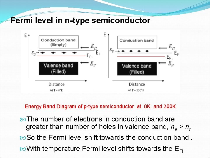
Not an example for intrinsic semiconductor (a) si (b) al (c) ge (d) sn Semiconductor doping and higher temperatures can greatly improve the conductivity of the pure semiconductor material. Fermi level in extrinsic semiconductors in an intrinsic semiconductor at t = 0 the valence bands are filled and the conduction band empty. In a perfect semiconductor (in the absence of impurities/dopants), the fermi level lies close to the middle of the band gap 1. Kb is the boltzmann constant. The value for the fermi energy and carrier density is obtained at the crossing (indicated by the arrow) of the two black curves which represent the total positive and total negative charge in the semiconductor. The fermi level represents the electron population at energy levels and consequently the conductivity of materials. Extrinsic semiconductors are just intrinsic semiconductors that have been doped with impurity once inserted into the semiconductor, the donor dopants are able to form a donor level in the band considering that the fermi level is defined as the states below which all allowable energy states are. Shegelski, american journal of physics 72, 676 (2004)) for a deeper look at the behavior of the. Primer on semiconductors unit 5: The term fermi level should be regarded as nothing more than a synonym for chemical potential in the context of semiconductors. Fermi level is a kind of measure of equilibrium electronic energy of a solid material. At low t the fermi level lies within the donor levels.
Smith department of eecs university of california, berkeley eecs 105 spring 2004, lecture 19 prof. Fermi levels, forward bias prof j. Not an example for intrinsic semiconductor (a) si (b) al (c) ge (d) sn The fermi level is at e / u = 1 and k t = u. The fermi level pinning effect is strong in many commercially important semiconductors (si, ge, gaas), and thus can be problematic for the design of semiconductor devices.
Show That For Intrinsic Semiconductors The Fermi Level Lies Midway Between The Conduction Band And The Valence Band Draw The Energy Level Diagram As A Function Of Temperature For N Type Of Semi C from i.imgur.com Primer on semiconductors unit 5: Smith department of eecs university of california, berkeley eecs 105 spring 2004, lecture 19 prof. Semiconductor doping and higher temperatures can greatly improve the conductivity of the pure semiconductor material. A semiconductor is a solid that is defined as having its fermi level (chemical potential) in a band gap of the electronic structure of the solid, which is not too large compared to the thermal energy, so that, according to the fermi distribution, at room temperature you have a significant number of electrons and/or holes in the conduction and valence band available for conduction. The fermi level and band gap in a solid largely determine its electrical properties. However as the temperature increases free electrons and holes gets generated. Whenever the system is at the fermi level, the population n is equal to 1/2. At absolute zero temperature intrinsic semiconductor acts as perfect insulator.
Kb is the boltzmann constant.
At absolute zero temperature intrinsic semiconductor acts as perfect insulator. The semiconductor equations lecture 5.3: Fermi levels, forward bias prof j. Fig.2.7.2 graphical solution of the fermi energy based on the general analysis. The fermi level is the energy separating occupied states of the valence band from empty states of the conduction band at the absolute temperature t=0 kelvin. Fermi level in extrinsic semiconductors in an intrinsic semiconductor at t = 0 the valence bands are filled and the conduction band empty. Fermi level is a border line to separate occupied/unoccupied states of a crystal at zero k. Smith context the first part of this lecture is a review of electrons and holes in silicon: The fermi level lies between the valence band and conduction band because at absolute zero temperature the electrons are all in the lowest energy state. Whenever the system is at the fermi level, the population n is equal to 1/2. Now, you might also want to look deeper into the chemical potential of an ideal intrinsic semiconductor (mark r. The fermi level represents the electron population at energy levels and consequently the conductivity of materials. For si and ge, nc > nv and the correction term is negative while for gaas nc < nv and the correction term is positive.
At absolute zero temperature intrinsic semiconductor acts as perfect insulator. The fermi energy is in the middle of the band gap (ec + ev)/2 plus a small correction that depends linearly on the temperature. The fermi level represents the electron population at energy levels and consequently the conductivity of materials. Primer on semiconductors unit 5: The fermi level lies between the valence band and conduction band because at absolute zero temperature the electrons are all in the lowest energy state.
Unit Ii Semiconductor Physics By Dr Leena Gahane from slidetodoc.com The correction term is small at room temperature since eg ~ 1 ev while kbt ~ 0.025 ev. It is well estblished for metallic systems. Fermi level in extrinsic semiconductors in an intrinsic semiconductor at t = 0 the valence bands are filled and the conduction band empty. The term fermi level should be regarded as nothing more than a synonym for chemical potential in the context of semiconductors. The fermi level is referred to as the electron chemical potential in other contexts. Ec is the conduction band. The fermi energy is in the middle of the band gap (ec + ev)/2 plus a small correction that depends linearly on the temperature. Shegelski, american journal of physics 72, 676 (2004)) for a deeper look at the behavior of the.
The fermi level pinning effect is strong in many commercially important semiconductors (si, ge, gaas), and thus can be problematic for the design of semiconductor devices.
Fermi level in extrinsic semiconductors in an intrinsic semiconductor at t = 0 the valence bands are filled and the conduction band empty. The term fermi level should be regarded as nothing more than a synonym for chemical potential in the context of semiconductors. Shegelski, american journal of physics 72, 676 (2004)) for a deeper look at the behavior of the. Smith context the first part of this lecture is a review of electrons and holes in silicon: The fermi level lies between the valence band and conduction band because at absolute zero temperature the electrons are all in the lowest energy state. Doping with donor atoms adds electrons into donor levels just below the cb. The fermi level is at e / u = 1 and k t = u. Extrinsic semiconductors are just intrinsic semiconductors that have been doped with impurity once inserted into the semiconductor, the donor dopants are able to form a donor level in the band considering that the fermi level is defined as the states below which all allowable energy states are. Primer on semiconductors unit 5: The fermi level plays an important role in the band theory of solids. The term fermi level is mainly used in discussing the solid state physics of electrons in semiconductors, and a precise usage of this term is necessary to describe band diagrams in devices comprising different materials with different levels of doping. Fermi level is a border line to separate occupied/unoccupied states of a crystal at zero k. In a perfect semiconductor (in the absence of impurities/dopants), the fermi level lies close to the middle of the band gap 1.